Only a short note. I made a video showing all the different PWM Schemes Open-BLDC supports. Have fun watching:
Cheers Esden
Only a short note. I made a video showing all the different PWM Schemes Open-BLDC supports. Have fun watching:
Cheers Esden
Hi!
As promised I made some videos. First one is showing the maiden run of a motor connected to the breadboard prototype of Open-BLDC.
(There is also a Vimeo version: Maiden Run of Open-BLDC from Piotr Esden-Tempski on Vimeo)
Yes the motor sounds like a truck. The reason is that I am making forced commutation (not detecting the right time to commutate but do it in fixed time) and the PWM duty cycle is higher then it should be. This way the motor is just jumping between the magnets and has a lot of vibrations.
The second video is a demo of sensorless commutation detection.
(There is also a Vimeo version: Open-BLDC Sensorless Commutation Detection Test from Piotr Esden-Tempski on Vimeo)
We are using a novel way without a virtual crosspoint. (you can read it up in this paper) We do it even a little bit differently then described in the paper, there are no comparators and latches. What we do is condition the signal to be in the range of 0V to 3.3V and sample it with the ADC at the right times. This is probably the simplest way to do something like this in the STM32. One can now play around with the data that the ADC delivers. I think there is a lot of stuff that can be done using such an approach.
In the video you may also wonder why it is so loud. Well the PC fan that I just forced onto the rotor is not really the best payload, also it is not balanced well and the bearings in the motor are not the best anymore because of the unbalanced load. ^^ I am also using the simplest and worst PWM scheme that I know of. The so called H PWM L ON scheme.

“H PWM L ON” PWM scheme. Click on the Image to see other PWM schemes.
You can also see in the video that the motor is pretty robust to external disturbances when running in the commutation detection closed loop. Still I am sure that it can be improved. (If you are interested the sourcecode running this can be seen here)
If I am not mistaken then only current measurement is missing in the circuitry. When that is done then I can design the first etched prototype of Open-BLDC. WOOO! 🙂
Cheers Esden
P.S. If you have any comments/ideas feel free to write them in the comment section. ^^
Hi!
It has been a pretty long time since my last post. But do not worry there is happening a lot “behind the scenes”. Well not so much behind them because I commit everything I do to the github repository (http://github.com/esden/open-bldc). If you want to follow the progress you can also subscribe to the commit mailinglist and/or the discussion mailinglist. Feel free to write on the mailinglist if you have any questions or just catch me on #uavp channel on the freenode network. (I think that are enough channels of communication 🙂 )
Ok back to the topic. Last week I was able to turn a bldc motor the first time using the bread board prototype of the power stage, the STM32 Olimex H103 evaluation board and firmware that you can find in the repository. The basic PWM scheme that is used by most controllers is implemented and works pretty well. I am also trying out other PWM schemes that may improve efficiency. You may ask why I am doing it now and not after I made a real hardware prototype of the system. The answer is pretty simple. I have to see if and how it is possible, to make sensorless commutation detection, when using different PWM schemes. I had to realize that the schemes have a big influence on the signals that can be captured.
As soon as I have more results I will make a video showing the current state and how the controller behaves when using different approaches. So stay tuned!
Cheers, and I hope hearing from you too in the comments! 🙂

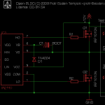
Circuit
For testing you can take a big capacitor, so that when you manually switch on the high side you see something happen. I took a 330uF capacitor and it is enough to turn the high side MOSFET on for about 30 seconds. Still you have to be careful because the capacitor only gets charged when the low side MOSFET is turned on. So after turning on the power the capacitor is not charged and you have to turn the low side MOSFET on first, then turn it off again and finally switch the high side on.
In the final design one should probably select the right bootstrap capacitor. The equation for calculating that value is described on page 6 of the International Rectifier application note AN-978.
You can probably get rid of the capacitor and the diode if you connect VCC directly to VB. The problem you get then is that when the current on VS gets higher then 12V you get a problem. But I may be mistaken. Correct me if I am wrong.
Conclusion: read the damn application notes and I still have problems with understanding the electrical engineer talk! 🙂
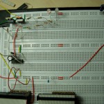
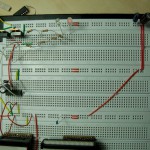
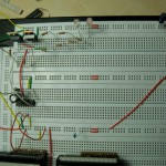
I hope this helps someone. You can see my circuit for one half bridge attached to this post. And a picture of my breadboard.
I use the two LEDs to see what happens with the MOSFETs. They are glowing a little when both sides are off. The one connected to 12V is switching off when the high side is on and the one connected to GND switches off when the low side is on. I love LEDs! 🙂
Cheers Esden
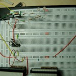
The other day I ordered parts to build the first prototype of Open-BLDC on a breadboard. It is a bit different animal then the board designs I already have because it needs legged parts.
The main problem is to find the right MOSFETs and driver chips for this application. As I have no electrical engineering background I did not really understand the values that were listed in the data sheets. I asked an electrical engineering friend and he helped me with locating the most important values. Thanks Federico!
I realized that the most important values for MOSFETs are:
The MOSFET I selected is not perfect but should do for this first prototype. It is the IRF1010N from International Rectifier.
Drain to source voltage
In my case as I am using the standard three cell LiPo batteries used in models. I need something above 12V. The smallest ones are 20V but the one I could get from Reichelt was 55V. That is still OK.
Gate to source voltage
For example the high side MOSFET has 12V attached to source. When the gate is driven low, the voltage difference between gate and source are 12V. In many cases that is a problem. Because when you charge your battery full the voltage difference gets even bigger or even worse when you try to use a battery with 4 cells instead of 3. Most MOSFET that I found have only 12V specified as gate to source voltage. It still probably works with more because of tolerances but still it is probably not good. The MOSFET I am now using for the prototype has ±20V in the specification. That should work.
Continuous drain current
This one will get more important in the future. It is telling how much current the MOSFET can put through. For the prototype that is more or less a functional test of the circuit it does not matter so much. But in the future when I want the controller to support up to 20A continuous current this one will get very important. The IRF1010N is specified for 85A at 25ºC and 60A at 100ºC. So this values are meant for applications where you have a heat sink attached to the MOSFET’s. I will try to avoid using heat sink. I could calculate the exact number but the rule of thumb is that one should take 1/10th of the value. This means that with this MOSFET I will be able to run at about 6A to 8A. As the lab power supply, I have access to and will use for the prototype, can only deliver 2A that should be more then enough. There are several other values that are connected to this one. Like drain to source on resistence, thermal resistence, power dissipation aso. One can use them to calculate the exact amount of current the part can put through. But I think it is too early to make all the calculations yet.
Input/Output capacitance (turn on/off time)
This is a set of values that tell how fast the MOSFET can be switched on and off. It will also get more important in the future when selecting the right MOSFET for the final design. For now the 76ns rise and 40ns fall times should be enough. They will probably get even lower because I am using a dedicated half bridge driver chip.
I did a lot less research here. Thankfully there are not as many half bridge drivers out there as there are MOSFETs. The one I selected is the IR2110. It would be a bit big for the final design because of the additional leads. But it should be OK for this prototype. The problem I had here is that I have 3.3V digital input from the microcontroller and I want to drive the MOSFETs with 12V. As it seems the other drivers that I considered don’t recommend that. That is why I had to choose this one. I hope that I will find something that is smaller and still supports the 3.3V input.
Selecting parts is a very tiresome endeavor. The shops only have a subset of the parts that are available out there. I wanted to order all parts from one shop that is somewhere in Germany. I could probably get better parts ordering from Digikey but it would cost more. For the next stage of Open-BLDC development I will have to select better parts. But first I how a feasible circuit should look like. That is why I am going for the breadboard test first.
If you find any mistakes or I misunderstood something here feel free to tell me.
Cheers Esden