THC RAM banks
Many parts in the schematic of THC have been based on the schematic of the S3CEV40 board schematic. This applies for example to the RAM wiring. I understood the overall idea but one detail was still a riddle to me, until yesterday.
As you can see in the following screenshot of the schematic the bank select pins BA0 and BA1 are connected through a set of 4 resistors to the address pins A21, A22 and A23 of the processor.
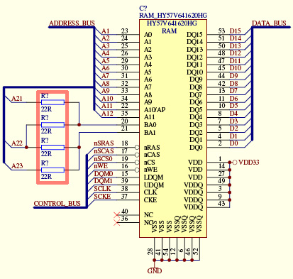
That is a strange setup, don't you think? Well, I dug into the documentation of the RAM chip and the processor and found out that when I am using an 8MB SDRAM chip with 4banks x 1MB x 16bit for S3C44B0X (the processor) I have to connect the address pins A21 and A22 to the bank select pins BA0 and BA1 of the RAM chip. But in case I want to use a 16MB chip with 4banks x 2MB x 16bit I have to connect the address pins A22 and A23 to the pins BA0 and BA1. !bam! finally I knew what was going on! The design of the evaluation board is made in such a way that you can put an 8MB or a 16MB RAM chip on it. And to match the address pin connection they put only two of the four resistors on the board to match the connection. I today checked that on the real board. Here is an image of the relevant part of the board.
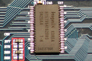
As you can see my thoughts were right. Only two of the four resistors are in place. In my case there is an 8MB RAM chip and so only the upper alterating pair of resistors is in place.
Yes it is pretty simple, I know. But when you look at the schematic you do not think about the purpose of such a set up at first. I am still learning to think in the terms of hardware design so this was a challenge for me.
There are still many riddles to be solved. One that I know of is the way the keypad on the eval board is connected to the chip. I will write about that when I know more about it.